Improvement of logic analyzer from China. Refinement of a logic analyzer from China Miniature 4-channel logic analyzer on avr
Vassilis Serasidis
A logic analyzer is a tool that allows you to see and analyze the sequence of logical 0s and 1s in a digital signal. For example, you can study digital signal from an IR receiver-demodulator type TSOP-1736, output and input signals of the microcircuit, as well as the I2C bus (clock line and data line) in many electronic devices.
In this article we will look at the design of a miniature 4-channel logic analyzer with an LCD display from mobile phone Nokia 5110/3110. The basis of the design is a microcontroller; in addition to it, several more discrete components are used.
Main characteristics of the device:
- 4-channel logic analyzer;
- the ability to study signals with a frequency of up to 400 kHz;
- input voltage up to +5 V;
- LCD display with a resolution of 84 × 48 pixels;
- powered by 4 batteries 1.2 V, maximum supply voltage 4.8 V;
- memory: from 3.7 ms for high-speed signals to 36 s for low-speed signals;
- control buttons;
- simple design.
Figure 1 shows a schematic diagram of the device. It should be immediately noted that the device is powered by 4 batteries with a voltage of 1.2 V each.
Attention!!!
Power supply from 4 batteries with a voltage of 1.5 V is unacceptable for this device circuit, since a voltage of 6 V can damage the microcontroller and LCD display.
Switch S1 is designed to supply power. Pull-up resistors R2-R5 are installed to prevent the appearance of false data at the digital inputs of the device due to the influence of electromagnetic fields or when fingers touch the signal probes. LED1 is designed to indicate the presence of a signal at the digital inputs of the device and, therefore, the start of recording signals into memory.
The circuit uses an LCD indicator from a mobile phone Nokia phone 3310/5510, it is designed to operate with a supply voltage of 3.3 V - 5.0 V, however, the maximum voltage for the display backlight is 3.3 V, so the circuit has three series-connected diodes (D1-D3) along the display backlight power line. Thanks to the diodes, the voltage will drop to 2.7 V and it will be quite enough to power the backlight.
Data capture process and software
It should be noted that the author has prepared two versions of the microcontroller firmware. Initially, for version 1.00 of the logic analyzer, an integrated development environment was used AVR Studio 4.18, but then the author recompiled source and for AVR Studio 5 - version 1.01. After recompiling for version 5 of the development environment and further testing the device, an improvement in the stability of the captured signals was noticed.
The signals are recorded into the internal RAM memory buffer, which is designed for 290 samples. The data buffer is formed by 870 bytes (for version 1 of the microcontroller program), of which 2 bytes are used for the counter and 1 byte for informing about the input channel. In version 1.01, the data buffer was reduced to 256×3=768 Bytes in order to increase the data capture speed, because The buffer size variable is 8-bit, instead of 16-bit, which was used in the first version of the software.
After power is applied, the microcontroller goes into pulse waiting mode at any of the 4 inputs of the device. By determining the input pulse, the microcontroller begins counting the time until the next pulse arrives at any of the 4 inputs. The sample duration is stored in the 16-bit variable “counter”. After this variable overflows, information about the state of the 4 inputs and the counter value are stored in a buffer and the value of its address is increased by three (2 bytes for the counter and 1 byte for information about the input line). This process is repeated until the microcontroller fills the entire buffer (870/3=290 samples or pulses). The process of recording signals into the microcontroller memory is shown in Figure 2.
After filling the buffer, all accumulated data is displayed on the LCD display in the form of an oscillogram. The user can control the waveform - move it to the left (S3 button) or to the right (S4 button) to view the entire saved pulse sequence. If low speed signals were recorded, the user can change the scale by 2, 4, 8, 16, 32, 64, 128, 256, 512, 1024, 2048, 4096 or 8192 by pressing the S2 button.
When programming the microcontroller, you must set the Fuse bits in accordance with the figure.

Type of printed circuit board and location of components


Demonstration of the device operation
Downloads
Schematic diagram, printed circuit board drawing, source code and file for microcontroller firmware (v1.0, AVR Studio 4.18) -
Source code and file for microcontroller firmware (v1.01, AVR Studio 5) -
- As I understand it, your display has a rubber band and is installed on a homemade scarf, i.e. the conductive rubber band touches the tracks that you cut on the scarf. If so, then keep in mind - this is the weakest point of the design... Have you checked (read) the Fuse bits? Are they installed correctly? I do not exclude the problem in the display itself. I'll take a look at the source code, maybe there is something that can be configured/changed regarding the display...
- Vadzz, yes, I understand that, the most vulnerable place.. I found some kind of mobile phone with a contact spacing similar to my screen. When I have time, I’ll try to do it.. The question is whether the screen is working, whether I burned its controller (if this is possible). In the meantime, I'll abandon this idea. It is very difficult to get this ready-made screen and it costs more than this device is needed.. I’d rather make the same device, only outputting data to a computer via USB. (according to the textbook http://eldigi.ru/site/comp/18.php). I still work on a computer and do everything via USB. Or a friend is doing a thesis on a miniature usb oscilloscope. Circuit based on a single AtTiny element and quartz. + output data to a program on a computer in the form of a time diagram/line.. I’ll take it from him.. I’ll make the software.. I started making this thing because it looks so beautiful and pretentious from the outside;) And it especially works.. well, nothing, I’ll start working with Chinese transmitters, I’ll have to do it.. There you already need to look at the impulses and analyze them.. And thanks for the help)
- Guys, check it out) Still, I couldn’t resist... I’m still thinking about finishing the front panel.
- I'm glad that everything turned out and worked, it looks normal. Just tell us in more detail what the problem was (probably the display didn’t work after all), your information will be useful for many (if it’s not a secret, of course). Thank you.
- Well the problem was in the display. And then I bought not red, but blue, so the contacts still do not agree on the location, and the names differ slightly. Connection (on the diagram\blue display): Vcc-Vcc GND-GND Rst-Rst SCE-CE D\C-DC DN-Din SKLK-CLK LED-BL If there is a desire, I will try to insert\start my old display. I'll see if it's burned out... otherwise I've had so much trouble with it.
- A small test of the device, a couple of bugs. 1) When rewinding, we move forward for a long time, then back, and at some point it refuses to move back and gets stuck at some value. You can scroll forward and back again and after that it jams at a different value.. Here is a photo, although nothing will be visible here http://s017.radikal.ru/i433/1306/57/cf1dfbd2f106.jpg 2) When rewinding, the temporary diagram http://s60.radikal.ru/i169/1306/33/1c23e0d9815c.jpg http://i066.radikal.ru/1306/9f/c894839ca1fd.jpg 3) When changing the zoom, rewinding is reset to the 0th position( but not always). We need to fix something... I think we could add a couple of goodies to the project: Touch buttons (implemented in a simple way, only three MOM resistors) Voltmeter (GND is constantly connected, so it would be nice to do something on the ADC, because it’s not the same to connect a multimeter every time , but this one would help. It measures up to 5V, just for a digital camera).
- Oscilloscope (I don’t know how, but it would be very nice. I think the main problem will be with the display).
- Connection via USB to PC. Displaying a time diagram in a program is sacred. If you make an oscilloscope, then it will be easier to display everything in the program.. It will look something like this (my program) http://s48.radikal.ru/i119/1306/eb/9c25ff0d3d7b.png You can also change something in the settings with the program device..
- By the way, this thing is simulated quite well in Proteus.
- I assembled the device. Turns on and shows. If there are 33k resistors (and no signal sources), then when you turn it on you can see all sorts of combs. With resistors and a source (TSOP IR and spi device) - all lines are even. No reaction at all. Where should we dig?
- The inputs are shorted to + and not to ground so that it shows. I had to invert the TSOP output.
- Firmware with corrected errors and with additions (UART, Frequency meter, Gap editor before measurement, as well as another program for the computer. Analizator.exe Description: Analizator_PC V2.1 Analizator.exe 4-channel logic analyzer. DSN Description: Analizator_proteus http:// www.fayloobmennik.net/4274643 Analizator.hex Description: Analizator_Atmega8 http://www.fayloobmennik.net/4291611 4-channel logic analyzer Description: Analizator_shema http://www.fayloobmennik.net/4285824 2nd option http://radikal.ru /fp/SOURCES FOR THE ANALYZER WHO IS INTERESTED. AnalizatorKSA.zip Don’t doubt everything works as it should! You will now have the opportunity to check it in the simulator, as well as delve into the source code. I’ll save you from routine work. Don’t judge me for my comments there. They are their own. Besides, these are drafts, not a commercial product. My goal was achieved, so the drafts remain drafts. You can do anything with them, even rip out their heart. And there was only one goal - to make it convenient, more accurate, and reliable. You can read everything that I have done in my 2 programs for PC in the “Help” section. To analyze and compare the results obtained, I am posting the source text of the main measuring program Vasilisa Serasidisa. Look and compare how many clock cycles are spent on measurement for me and for him. And make sure that the best programmers are RUSSIAN!!! I’ll add: Since I designed 2 versions of the analyzers, I’ve solved many problems related to digital exchange via the CAN bus and I2C consoles, etc. The ATmega48 version is even preferable with high-speed protocols. For example, CAN of 140 Kbit was analyzed simply with a bang! in contrast to the well-known Digan analyzer. And he himself is the size of a flash drive. Good luck to all! Izmerenie.txt I AM POSTING A NEW VERSION (3rd version) OF A MORE POWERFUL ANALYZER, AS WELL AS THE PREVIOUS VERSION WITH ADDES AND PROTEUS FILE LINK TO ARCHIVE http://www.fayloobmennik.net/5569369
- 1. Who repeated the original version - from Serads, are there any serious bugs that make the device inapplicable at all - like the first byte is always skipped, etc.? Above they write about “displaying diagrams”, but I would like that they were reliable :). 2. Sergey7 does not post the source code, which does not allow us to fully evaluate its functionality. If you make the original first, will changes in the hardware be required for further development of the device to finalize Sergei7?
- I sent you a message and no response. Has it arrived?
- probably not. ... :(Thanks for the sources! I'll take a look in a minute.....
- Glad to help! :D
- Firmware with additions (UART, Frequency meter, Gap editor before measurement is not in AnalizatorKSA.zip
- Maybe someone has a signet in lay?
- Look at the new version I posted. And the previous one, modified too (with firmware, proteus file and additional program).
- What did they write in and can I have a complete diagram? I still don’t understand what to collect and how many other percents it writes to itself for transmission via UART
This article presents a simple logic analyzer that works with the USBee v1.1.57 and Logic v1.1.15 shells. Assembled on a common microcircuit CY7C68013A from Cypress. I had a ready-made board with this chip, ordered from the Aliexpress website. This is what she looks like:
I wanted to make an LPT port on it, but then the need for it disappeared and so it lay around unclaimed. I needed a simple logic analyzer. It was decided to do it on this board. There are many circuits based on this chip on the Internet. It was necessary to add a buffer for data transfer, provide input protection and the ability to choose which shell to work with. The expansion board is placed on top of the main board. I will say right away that the circuit, board, firmware and everything necessary to work with this logic analyzer is at the bottom of the article. The 74LVC4245 chip was used as a buffer; you can use the 74LVC8T245A; they are completely identical. The protective function at the input is performed by BAV99 diode assemblies. And so this scheme was born:

Use jumper J1 to select the direction of data transfer. In the closed state for data reception, in the open state for transmission. There is such a shell as USBee AX Test Pod. It contains many test utilities that can be used to test the operation of the assembled device. One possibility is to generate different frequencies on the XP3 pins. True, you can’t ask them yourself. 8 different frequencies are displayed at once. You can also set outputs to 0 or 1 and many other tests. Use the XP5 jumper to select which shell we will work with USBee v1.1.57 or Logic v1.1.15. Firmware for different shells is respectively loaded into U2 and U3. The XP4 jumper is write protected. It will be needed when starting the Logic shell. Jumper J2 sets the voltage of the input levels. If it is closed, then the input signal level should be 3.3 V. It is also possible to set the signal level to the same voltage as the voltage being supplied to the device being diagnosed, but not more than 5V. To do this, open J2 and apply the supply voltage to the board being diagnosed to pin 10 of XP3. Also, do not forget to connect the common wire of the analyzer with the board being diagnosed. First, we need to modify the main board, that is, remove the 24C128 memory chip.
My board also did not have a GND connection between the USB connector and GND CY7C68013A had to be wired together.

No further changes need to be made.
Now we make our scarf measuring 41mm x 58mm. As a result, we get the following result:


We connect two boards:


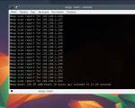
To get started, we need to flash the memory chips. To do this, install the utility from Cypress CySuiteUSB_3_4_7_B204. We remove the XP5 jumper from the board and connect the board to the PC, an unknown device will appear in the device manager.

Install drivers from the file Driver_Cypress_win7 win8. We tell the dispatcher to look for drivers in this folder. The system will install the necessary driver itself. A new device will appear in the USB controllers:

Launch the installed program Control Center. A window will open in front of us, where our device should be at the top.

Select the Option tab then EZ-USB Interface:

The following window will open:

We are not changing anything here. We only need the S EEPROM button. Use the XP5 jumper to select one of the memory chips. Click S EEPROM and indicate where our firmware is stored. Select the firmware depending on the type of memory and click "Open". The numbers at the end of the firmware name indicate what type of memory the firmware is for. For 24C01 you need to select USBeeAX_01, and for 24C02 USBeeAX_01.

The process of uploading information will begin. If the firmware is successfully installed, there should be a message like in the screenshot. The number of bytes may vary depending on the selected firmware.

We press the reset button on the board and see a new unidentified device in the device manager. Installing drivers. IN automatic mode the drivers will not be installed. In manual mode, we indicate what to install from the disk and select the driver from the Driver Cypress win7_win8 folder. It worked for me on Windows 8.1 with the EZ-USB FX1 No EEPROM driver (3.4.5.000).
When buying all sorts of Chinese electronics for my “crafts,” I often encounter the problem of a poor description of the work,
The topic of today's article is the use of a cheap Chinese logic analyzer purchased on Aliexpress.
What is a logic analyzer? This is such a device... for logical analysis))) A film with Robert De Niro immediately comes to mind

Why is it needed? Well, of course, engage in logical analysis))). Or rather, by analyzing the logical levels of different microcontrollers and their peripherals. What is commonly called reverse engineering.
Characteristics
- Software compatibility with Saleae Logic 8
- Number of digital inputs - 8
- Two indicators - power and logical input status
- Input impedance 100KOhm, input capacitance 5pF
- USB Powered
- Supported sampling rates:
- 24MHz,16MHz, 12MHz, 8MHz, 4MHz, 2MHz, 1MHz, 500KHz, 250KHz, 200KHz, 100KHz, 50KHz, 25KHz;
- Number of stored values of one measurement - 10000


On one side there is a 10-pin connector and pinout on the body
With another Mini USB for power supply and connection to a computer

Entrails
Inside the case there is a board containing a microprocessor with a high-speed USB interface CY7C68013A from CYPRESS, an EEPROM ATMLH432 and a bus driver LVC245A from NXP.


At the analyzer input there are 100 Ohm current-limiting resistors, 100 KOhm pull-up resistors and 5 pF capacitors. Everything is honest, as in the description.
Connection
To connect the analyzer, the kit includes 10 connecting wires for pin contacts. I immediately bought these clip-on clips.

The quality of the clamps is very mediocre, but good clamps will cost more than the analyzer itself


Software
This is perhaps the most interesting thing about this analyzer. It comes with native software from Saleae Logic.
Versions are available for OSX, Linux and Windows in 32 and 64 bits.
Saleae Logic 1.2.3 under Windows 7 worked with half a kick, the software started, the hardware was recognized, despite the “Beta” version sign.
Interesting features in software from Saleae Logic
Trigger for recording a logical sequence on each channel
- To change the logical level to “0”
- To change the logical level to “1”
- For a positive impulse of a given duration
- To a negative pulse of a given duration
Calculation of statistical readings based on the current measurement
Decoding protocols: Async Serial, I2C, SPI, Hide, 1-Wire, Atmel SWI, BISS C, CAN, DMX-512, HD44780, HDLC, HGMI CEC, I2S/ PCM, JTAC, LIN, MDIO, Manchester, Midi, Modbus , PS/2 Keyboard/Mouse, SMBus, SWD, Simple Parallel, UNI/O, USB LS and FS
Logging using decodable protocol
In addition, this analyzer can be flashed with software from USBee
Let's do some analysis

I was just figuring out connecting the DYP-ME007Y ultrasonic sensors, which look absolutely identical, but work completely differently.

If one works exactly according to the datasheet: a short pulse on the “trigger” triggers an ultrasonic pulse and the distance is measured by the duration of the echo. Then the second and third (with a blinking LED) approximately once every 100ms without any external kicks measure the distance and send it at a speed of 9600 in the form of four bytes (including checksum). Saleae Logic allows you to enable signal decoding serial bus into a sequence of bytes. Sensors of the second type work perfectly with the “TRIG” output disabled, although they may be waiting for some kind of command at this input, but even a magic device will not show this.

Next, you wanted to look at the PWM signal of Atmegi 168? I turned on all six channels supporting PWM at different levels and was surprised to find that the frequency of two PWM channels differs from the other 4. Are different timers involved?


What's on my data bus?

The magic device and the program normally decoded the sequence output to the LEDs. Even the colors of the LEDs appeared.

There are no problems with analyzing the I2C bus either. The software coped well with decoding. You can see write packets to registers when the TM1637 display driver is running

A 315 MHz RF receiver connected directly to the analyzer received a signal from the radio switches and issued a Manchester code. After selecting the speed, the Manchester code is converted by a smart program into a sequence of bytes.

I wonder, what about the accuracy of measuring time intervals? I didn’t have an exact pulse generator at hand, but Arduino tone(1000) at 1000Hz

and tone(20000) at 20KHz give a fairly accurate result.

To test the high frequency, I quickly assembled a generator based on the NE555. We managed to squeeze 8 MHz out of it. The analyzer absorbed this frequency normally. It was not possible to test it at 20 MHz, but 8 is also a very good result for such a cheap piece of hardware.
A short summary
A logic analyzer is a very necessary and useful thing for those who are engaged in digging up Chinese peripherals for microcontrollers (Let's call it nicely - reverse engineering)
Among the advantages of this piece of iron I would like to note:
- Attractive price
- Compatible with quite convenient Saleae Logic software
- Input protection in the form of LVC245A bus driver
- Small dimensions
I didn’t find any obvious shortcomings in this piece of hardware. I wish I had purchased a logic analyzer sooner - how much time I would have saved on so many projects. Undoubtedly, for some, the capabilities of this piece of hardware will not be enough. There are a lot of more sophisticated models, but the price of $100-200 makes these devices much less affordable for radio amateurs.
Shall we analyze anything else?

To work in complex digital circuits, a Chinese logic analyzer is an extremely necessary thing. Its low price and convenient software are also captivating. And it suited me quite well until the need arose to simultaneously view the operation of different circuit nodes, powered from different sources and not having a common ground. Initially, the analyzer has 8 power-uncoupled channels with a pulse amplitude at the input of 5 volts. This modification makes it possible to make the analyzer inputs galvanically isolated and work with pulses with an amplitude from 3 volts to 25 volts. The position of the biscuit switches is selected depending on the range of the input pulses. But the design circuit will remain operational up to 65 volts.
The circuit uses high-speed optocouplers designed to operate in fiber optic networks. The frequency characteristics of the optocoupler are higher than the analyzer can miss, since the minimum pulse duration that the analyzer can register is something like 42 nanoseconds. The optocoupler LED current is selected in the region of 6-7.5mA. The optocoupler allows the current to increase up to 15mA. And such a current will arise at an input voltage of 65 volts when the switch is in the “25v” position.

Specifically, my board contains 4 galvanically isolated channels and 4 non-isolated ones with 5-volt inputs. Power is supplied from the analyzer board. In this case, it is necessary to carry out some modifications: remove the analyzer board from the case, cut the track going to pin 9 of the connector and apply voltage from the right pin of LM1117 to this pin through a 10 Ohm resistor.

The layout and design turned out to be quite simple, and the possibilities of use were significantly increased.
When testing galvanically isolated inputs, for the purity of the experiment, the inputs were connected in parallel. That is, 4 inputs IN A,B,C,D and, accordingly, Gnd A,B,C,D were mutually connected. The switches were set to the same position. The pulses were created by artificial bouncing of contacts and an external power source at the appropriate voltage.


During assembly, 6N137 optocouplers and MPN-1 switches were used; the dividers contain smd0805 resistors, but 1206 will also fit. When soldering the cable for connection to the analyzer, the sequence was partially changed, but everything is labeled on the board.
Instead of MPN-1 switches, you can use any others, although you will have to adjust the printed circuit board or use wires. Author - Dubovitsky Nikolay.
Main characteristics of the device:
- up to 32 input channels;
- memory 128 KB per channel;
- sampling frequency up to 100 MHz;
- external clock input;
- all inputs are compatible with 3.3 V and 5 V logic;
- configurable prefetch/postfetch buffer size is a multiple of 8 KB;
- 16-bit internal clock generator;
- several internal synchronization modes;
- programmable sync delay;
- programmable synchronization event counter;
- external synchronization input;
- communication with PC via LPT (EPP mode) or USB interface;
- Several versions of PC applications for various operating systems.
The main element of the logic analyzer is the FPGA, produced by the company, which performs all the main functions. The schematic diagram of the device is shown in Figure 1.
Oscillator IC4 (IC6), borrowed from the old one, is used as a clock source for the FPGA motherboard computer. Despite the fact that the oscillator is designed to operate at a voltage of 5 V, no problems were identified in the operation of the device when powered by a voltage of 3.3 V.
An external high-speed RAM chip is used to store samples.
To power the device it is used external source with an output voltage of up to 15 V. The FPGA and RAM have a supply voltage of 3.3 V, so a 3.3 V voltage regulator of the LD1117DT33 series is installed.
The K7 parallel port connector is located on the logic analyzer board and is connected directly to the FPGA. The logic analyzer's circuit board is double-sided, using surface mount components and conventional leaded components. A view of the printed circuit board is shown in Figure 2.
Comment. Instead of pin 40 (Vss) of the SRAM chip, pin 39 of this chip is connected to ground. Solution: Connect pins 39 and 40 together on the PCB (pin 39 is not used in the SRAM chip).
To connect to personal computer For the USB interface, you must use a special adapter, the diagram of which is shown in Figure 3.
The USB interface adapter for the logic analyzer is assembled on a FT2232C series chip manufactured by FTDI. This chip combines the functionality of two separate chips FT232BM and FT245BM. It has two I/O channels that are separately configured. The main points of the FT2232C configuration for use as part of the device are power supply from the USB interface and microcontroller bus emulation mode (MCU Host Bus Emulation mode). This mode is converted to the EPP protocol using the IC3 74HCT4053D multiplexer. Since direct decoding of the /DST, /AST and RD/WR signals can cause timing conflicts, an additional signal A8 is used, which is used as an RD/WR (read/write) signal during periods of data transmission via the EPP protocol.
The JTAG connector (CON2) is used to configure the FPGA - this is for future development, at the moment this interface is not used.
The 93LC56 series EEPROM (IC2) stores configuration data for the FT2232C and is required for the programmable interface to function properly. To program this chip, the FT_Prog utility is used (previously it was called MProg). This utility and FT2232C drivers are available for download on the FTDI website.
The adapter printed circuit board is designed single-sided, which simplifies its manufacture.
There is also version B 1.0 USB adapter interface (Figure 5). This version differs in the absence of a JTAG connector and printed circuit board, which is made taking into account its integration into the body of the CANNON 25 connector. Appearance assembled adapters in Figure 6.
  |
|
| a) | b) |
| Figure 6. | Appearance of the USB interface adapter version A 1.1 (a) and version B 1.0 (b) |
There is also another version of the logic analyzer circuit (Figure 7), into which USB and LPT interfaces are already integrated. The author of this option is Bob Grieb and when developing the circuit, the TinyCAD environment was used, the printed circuit board for it was developed in the FreePCB editor.