Choosing the optimal memory for a laptop: OCZ Value Series. Test configuration and overclocking technique
Part 26: OCZ Titanium and SLI-Ready series high-speed modules (PC2-6400, PC2-7200 and PC2-8000)
We continue to explore the critical characteristics of high-speed DDR2 modules using a universal test suite. Today we will look at high-speed offers from OCZ - three dual-channel 2 GB sets of memory modules of the Titanium and SLI-Ready series of speed categories PC2-6400, PC2-7200 and PC2-8000:
- OCZ DDR2 PC2-6400 Titanium EPP-Ready (OCZ2T8002GK, DDR2-800 4-4-4-1T)
- OCZ DDR2 PC2-7200 SLI-Ready Edition (OCZ2N900SR2GK, DDR2-900 4-4-3-2T)
- OCZ DDR2 PC2-8000 Titanium Alpha VX2 (OCZ2TA1000VX22GK, DDR2-1000 4-4-4-2T)
Module manufacturer: OCZ Technology
Module chip manufacturer: unknown
Module manufacturer website: Module appearance
OCZ DDR2 PC2-6400
OCZ DDR2 PC2-7200

OCZ DDR2 PC2-8000

Part Number of modules
There is no manual for decoding the Part Number of DDR2 memory modules on the manufacturer's website (during its study, only an outdated manual dedicated to DDR memory modules was discovered). Therefore, we will limit ourselves only brief description modules presented on the respective product pages.
OCZ DDR2 PC2-6400

The modules support the EPP standard, which allows for optimal module performance on motherboards with NVIDIA nForce 590 SLI chipsets. The EPP content is programmed for DDR2-800 mode with fairly low timings 4-4-4-1T, i.e. The modules are capable of operating at command interface delays of 1T (1 command/1 clock cycle), which significantly increases the performance of the memory subsystem. The modules are equipped with titanium-coated XTC (Xtreme Thermal Convection) heat sinks for efficient heat dissipation.
OCZ DDR2 PC2-7200

The modules also support the EPP standard, while the contents of this part of the SPD chip are programmed for DDR2-900 mode with a 4-4-3 timing scheme. According to the manufacturer, these modules are equipped with the exclusive NVIDIA XTC heat dissipation system (in terms of both efficiency and appearance, “corresponding” to the performance level of the modules).
OCZ DDR2 PC2-8000

Unlike the first two representatives, there is no support for the EPP standard in the modules. The modules belong to a special family of Voltage Xtreme modules, designed to operate at high supply voltages (allowing them to achieve speeds that are not possible at conventional voltage levels). This model designed for DDR2-1000 mode at 4-4-4 delays, which is achieved by raising the supply voltage to 2.3V and is positioned as a high-end solution for extreme gamers and overclockers. The heat dissipation of XTC modules using scratch-resistant titanium coating is also an exclusive solution, this time in its color scheme (see photo). Each Titanium Alpha module has a unique color scheme and changes its color shade depending on lighting and viewing angle. SPD module chip data
Description of the general SPD standard:
Description of the specific SPD standard for DDR2:
Description of EPP standard:
OCZ DDR2 PC2-6400
| Parameter | Byte | Meaning | Decoding |
|---|---|---|---|
| Fundamental memory type | 2 | 08h | DDR2 SDRAM |
| 3 | 0Eh | 14 (RA0-RA13) | |
| 4 | 0Ah | 10 (CA0-CA9) | |
| 5 | 61h | 2 physical banks | |
| 6 | 40h | 64 bit | |
| Supply voltage level | 8 | 05h | SSTL 1.8V |
| 9 | 25h | 2.50 ns (400.0 MHz) | |
| Module configuration type | 11 | 00h | Non-ECC |
| 12 | 82h | ||
| 13 | 08h | x8 | |
| 14 | 00h | Undefined | |
| 16 | 0Ch | BL = 4.8 | |
| 17 | 04h | 4 | |
| 18 | 38h | CL = 5, 4, 3 | |
| 23 | 30h | 3.00 ns (333.3 MHz) | |
| 25 | 37h | 3.70 ns (270.3 MHz) | |
| 27 | 32h | 12.5 ns 5.00, CL = 5 4.17, CL = 4 3.37, CL = 3 |
|
| 28 | 28h | 10.0 ns 4.00, CL = 5 3.33, CL = 4 2.70, CL = 3 |
|
| 29 | 32h | 12.5 ns 5.00, CL = 5 4.17, CL = 4 3.37, CL = 3 |
|
| 30 | 25h | 37.0 ns 14.80, CL = 5 12.33, CL = 4 10.00, CL = 3 |
|
| 31 | 80h | 512 MB | |
| 36 | 3Ch | 15.0 ns 6.00, CL = 5 5.00, CL = 4 4.05, CL = 3 |
|
| 37 | 1Eh | 7.5 ns 3.00, CL = 5 2.50, CL = 4 2.02, CL = 3 |
|
| 38 | 1Eh | 7.5 ns 3.00, CL = 5 2.50, CL = 4 2.02, CL = 3 |
|
| 41, 40 | 37h, 00h | 55.0 ns 22.00, CL = 5 18.33, CL = 4 14.86, CL = 3 |
|
| 42, 40 | 69h, 00h | 105.0 ns 42.00, CL = 5 35.00, CL = 4 28.38, CL = 3 |
|
| 43 | 80h | 8.0 ns | |
| SPD revision number | 62 | 23h | Revision 2.3(?) |
| Checksum byte 0-62 | 63 | BFh | 191 (correct) |
| 64-71 | 7Fh, 7Fh, 7Fh, 7Fh, B0h | OCZ | |
| Module Part Number | 73-90 | - | OCZ2T8001G |
| Module production date | 93-94 | 06h, 26h | 2006, 38 week |
| Module serial number | 95-98 | 00h, 00h, 00h, 00h | Undefined |
According to SPD, the supported CAS# signal delay values are 5, 4 and 3. The first value (CL X = 5) corresponds to a clock period of 2.5 ns (frequency 400 MHz), i.e. DDR2-800 mode. The timing scheme for this case is not entirely represented by integer values and can be written as 5-5-5-14.8, which, taking into account the most likely rounding up, corresponds to the standard scheme 5-5-5-15. The reduced CAS# delay value (CL X-1 = 4) corresponds to the DDR2-667 mode (cycle time 3.0 ns, frequency 333.3 MHz) with a non-integer timing scheme 4-4.17-4.17-12.33, which, taking into account rounding, can be written as 4- 5-5-13. Finally, the twice reduced CAS# latency (CL X-2 = 3) corresponds to a somewhat erroneous but common recording of the DDR2-533 mode with a cycle time of 3.7 ns (frequency 270.3 MHz) instead of the nominal value of 3.75 ns (frequency 266.7 MHz). The timing scheme for this case is 3-3.37-3.37-10, taking into account rounding - 3-4-4-10.
The manufacturer identification code, manufacturing date and Part Number of the module are correct, while information about serial number module is missing. In addition, the strange meaning of revision SPD 23h, which formally corresponds to the non-existent revision number of the standard “2.3,” is somewhat alarming.
Since these modules support the EPP extension, let's now look at the information contained in this "non-standard" part of the SPD, represented by bytes 99-127 of the SPD content.
| Parameter | Byte(s) (bits) | Meaning | Decoding |
|---|---|---|---|
| EPP identification string | 99-101 | 4E566Dh | Supports SPD EPP |
| Profile type EPP | 102 | A1h | Short profiles |
| 103 (1:0) | 00h | Profile 0 | |
| Profiles used | 103 (7:4) | 01h | Profile 0: present Profile 1: none Profile 2: none Profile 3: none |
| Profile No. 0 | |||
| Supply voltage level | 104 (6:0) | 08h | 2.0V |
| Address transmission delay (Addr CMD rate) | 104 (7) | 00h | 1T |
| Cycle time (tCK) | 105 | 25h | 2.50 ns (400.0 MHz) |
| Delay CAS# (t CL) | 106 | 10h | 4 |
| Minimum delay between RAS# and CAS# (t RCD) | 107 | 28h | 10.0 ns (4.0) |
| Minimum time for recharging data in a row (t RP) | 108 | 28h | 10.0 ns (4.0) |
| Minimum pulse duration of the RAS# signal (t RAS) | 109 | 25h | 37.0 ns (14.8) |
EPP information is presented in the form of abbreviated profiles, the maximum possible number of which is 4, while in reality there is data only on the first of these profiles (profile No. 0), which, of course, is marked as “optimal”. The information contained in this abbreviated profile is very limited and is fully presented in the table above. This is data on the module supply voltage - 2.0 V, command interface delay (1T), cycle time (2.5 ns, memory bus frequency 400 MHz, DDR2-800 mode) and standard timings (4-4-4-14.8, taking into account rounding 4-4-4-15). Extra options fine tuning of the timing and electrical characteristics of the functioning of the memory subsystem is absent in the contents of the “reduced” EPP profile, which, in our opinion, casts doubt on its main advantages. Probably the module manufacturer simply did not pay enough attention fine tuning these characteristics. We will see what this led to further in the course of our study of the modules, but for now let’s move on to considering the SPD of the next representative.
OCZ DDR2 PC2-7200
| Parameter | Byte | Meaning | Decoding |
|---|---|---|---|
| Fundamental memory type | 2 | 08h | DDR2 SDRAM |
| Total number of module line address lines | 3 | 0Eh | 14 (RA0-RA13) |
| Total number of module column address lines | 4 | 0Ah | 10 (CA0-CA9) |
| Total number of physical banks of the memory module | 5 | 61h | 2 physical banks |
| External memory module data bus | 6 | 40h | 64 bit |
| Supply voltage level | 8 | 05h | SSTL 1.8V |
| Minimum duration of the clock period (t CK) at maximum delay CAS# (CL X) | 9 | 25h | 2.50 ns (400.0 MHz) |
| Module configuration type | 11 | 00h | Non-ECC |
| Type and method of data regeneration | 12 | 82h | 7.8125 ms - 0.5x reduced self-regeneration |
| Width of the external data bus interface (type of organization) of the memory chips used | 13 | 08h | x8 |
| Width of the external data bus interface (type of organization) of the ECC module memory chips used | 14 | 00h | Undefined |
| Duration of transmitted packets (BL) | 16 | 0Ch | BL = 4.8 |
| Number of logical banks of each chip in the module | 17 | 04h | 4 |
| Supported delay lengths CAS# (CL) | 18 | 38h | CL = 5, 4, 3 |
| Minimum clock period duration (t CK) with reduced CAS# delay (CL X-1) | 23 | 3Dh | 3.75 ns (266.7 MHz) |
| Minimum clock period duration (t CK) with reduced CAS# delay (CL X-2) | 25 | 00h | Undefined |
| Minimum time for recharging data in a row (t RP) | 27 | 32h | 12.5 ns 5.00, CL = 5 3.33, CL = 4 Undefined, CL = 3 |
| Minimum delay between activation of adjacent rows (t RRD) | 28 | 1Eh | 7.5 ns 3.00, CL = 5 2.00, CL = 4 Undefined, CL = 3 |
| Minimum delay between RAS# and CAS# (t RCD) | 29 | 32h | 12.5 ns 5.00, CL = 5 3.33, CL = 4 Undefined, CL = 3 |
| Minimum pulse duration of the RAS# signal (t RAS) | 30 | 25h | 37.0 ns 14.80, CL = 5 9.87, CL = 4 Undefined, CL = 3 |
| Capacity of one physical memory bank | 31 | 80h | 512 MB |
| Recovery period after recording (t WR) | 36 | 3Ch | 15.0 ns 6.00, CL = 5 4.00, CL = 4 Undefined, CL = 3 |
| Internal delay between WRITE and READ commands (t WTR) | 37 | 1Eh | 7.5 ns 3.00, CL = 5 2.00, CL = 4 Undefined, CL = 3 |
| Internal delay between READ and PRECHARGE commands (t RTP) | 38 | 1Eh | 7.5 ns 3.00, CL = 5 2.00, CL = 4 Undefined, CL = 3 |
| Minimum row cycle time (t RC) | 41, 40 | 37h, 00h | 55.0 ns 22.00, CL = 5 14.86, CL = 4 Undefined, CL = 3 |
| Period between self-regeneration commands (t RFC) | 42, 40 | 69h, 00h | 105.0 ns 42.00, CL = 5 28.38, CL = 4 Undefined, CL = 3 |
| Maximum duration of the clock period (t CK max) | 43 | 80h | 8.0 ns |
| SPD revision number | 62 | 12h | Revision 1.2 |
| Checksum byte 0-62 | 63 | 2Ah | 42 (correct) |
| JEDEC Manufacturer Identification Code | 64-71 | 7Fh, 7Fh, 7Fh, 7Fh, B0h | OCZ |
| Module Part Number | 73-90 | - | OCZ2N900SR1G |
| Module production date | 93-94 | 00h, 00h | Undefined |
| Module serial number | 95-98 | 00h, 00h, 00h, 00h | Undefined |
Supported CAS# signal delay values are 5, 4 and 3, however, the values of the clock periods are indicated only for the first two values: main (CL X = 5) and reduced (CL X-1 = 4). The first value (CL X = 5) corresponds to a clock period of 2.5 ns (frequency 400 MHz), i.e. DDR2-800 mode. The timing scheme for this case can be written as non-integer values 5-5-5-14.8, taking into account the most likely rounding up - 5-5-5-15. The second value (CL X-1 = 4) corresponds to the somewhat outdated DDR2-533 mode (cycle time 3.75 ns, frequency 266.7 MHz) with a non-integer timing scheme 4-3.33-3.33-9.87, which, taking into account rounding, can be written as 4-4 -4-10. As we noted above, the twice reduced value of the CAS# delay (CL X-2 = 3) does not correspond to any meaningful mode of operation of the modules, which is definitely an error.
The manufacturer's identification code and Part Number of the module are correct, but information about the date of manufacture and serial number of the modules is missing. These modules also support EPP extensions, so we will review the information contained in this part of the SPD below.
| Parameter | Byte(s) (bits) | Meaning | Decoding |
|---|---|---|---|
| EPP identification string | 99-101 | 4E566Dh | Supports SPD EPP |
| Profile type EPP | 102 | B1h | Advanced Profiles |
| Optimal Performance Profile | 103 (1:0) | 01h | Profile 1 |
| Profiles used | 103 (7:4) | 03h | Profile 0: present Profile 1: present |
| Profile No. 0 | |||
| Supply voltage level | 104 (6:0) | 14h | 2.3V |
| Address transmission delay (Addr CMD rate) | 104 (7) | 01h | 2T |
| Cycle time (tCK) | 109 | 22h | 2.20 ns (454.5 MHz) |
| Delay CAS# (t CL) | 110 | 10h | 4 |
| Minimum delay between RAS# and CAS# (t RCD) | 111 | 23h | 8.75 ns (3.98) |
| Minimum time for recharging data in a row (t RP) | 112 | 19h | 6.25 ns (2.84) |
| Minimum pulse duration of the RAS# signal (t RAS) | 113 | 21h | 33.0 ns (15.00) |
| Recovery period after recording (t WR) | 114 | 28h | 10.0 ns (4.55) |
| Minimum row cycle time (t RC) | 115 | 32h | 50.0 ns (22.73) |
| Profile No. 1 | |||
| Supply voltage level | 116 (6:0) | 14h | 2.3V |
| Address transmission delay (Addr CMD rate) | 117 (7) | 01h | 2T |
| Cycle time (tCK) | 121 | 22h | 2.20 ns (454.5 MHz) |
| Delay CAS# (t CL) | 122 | 10h | 4 |
| Minimum delay between RAS# and CAS# (t RCD) | 123 | 21h | 8.25 ns (3.75) |
| Minimum time for recharging data in a row (t RP) | 124 | 19h | 6.25 ns (2.84) |
| Minimum pulse duration of the RAS# signal (t RAS) | 125 | 1Fh | 31.00 ns (14.09) |
| Recovery period after recording (t WR) | 126 | 30h | 12.00 ns (5.45) |
| Minimum row cycle time (t RC) | 127 | 2Ch | 44.00 ns (20.00) |
The contents of the EPP look quite interesting. Unlike the OCZ DDR2 PC2-6400 modules discussed above with “reduced” EPP profiles, the OCZ DDR2 PC2-7200 modules in question contain in their EPP part information about two “extended” profiles (No. 0 and No. 1), both of which are valid , but correspond... to approximately the same mode of operation(!), apart from minor differences. Namely, in both profiles, the operating mode of the modules is “DDR2-900” mode (frequency - approximately 454.5 MHz, cycle time 2.2 ns) with a supply voltage of 2.3 V (which corresponds to the manufacturer’s specifications) and a command interface delay value of 2T. Only the main memory timing schemes differ somewhat, which in the first case can be represented as 4-3.98-2.84-15 (4-4-3-15 when rounded up), and in the second - as 4-3.75-2.84-14.09 . When rounding these values, we also get a 4-4-3-15 scheme (coinciding with that declared by the manufacturer), however, the EPP profiles also differ somewhat in the values of “other” timings like t WR and t RC. Be that as it may, profile No. 1 was chosen as the “optimal” profile.
The SPD contents of the OCZ DDR2 PC2-7200 modules under review (including EPP extensions) are clearly different from the SPD (and EPP) contents of the OCZ DDR2 PC2-6400 modules discussed above. One way or another, in both cases there are inaccuracies, and even obvious errors. Thus, OCZ's approach to programming SPD data turns out to be very peculiar, if not very careless. Finally, let’s look at the SPD contents of the latest representative - OCZ DDR2 PC2-8000 modules, which is represented only by the “standard” part due to the lack of support for EPP extensions.
OCZ DDR2 PC2-8000
| Parameter | Byte | Meaning | Decoding |
|---|---|---|---|
| Fundamental memory type | 2 | 08h | DDR2 SDRAM |
| Total number of module line address lines | 3 | 0Eh | 14 (RA0-RA13) |
| Total number of module column address lines | 4 | 0Ah | 10 (CA0-CA9) |
| Total number of physical banks of the memory module | 5 | 61h | 2 physical banks |
| External memory module data bus | 6 | 40h | 64 bit |
| Supply voltage level | 8 | 05h | SSTL 1.8V |
| Minimum duration of the clock period (t CK) at maximum delay CAS# (CL X) | 9 | 25h | 2.50 ns (400.0 MHz) |
| Module configuration type | 11 | 00h | Non-ECC |
| Type and method of data regeneration | 12 | 82h | 7.8125 ms - 0.5x reduced self-regeneration |
| Width of the external data bus interface (type of organization) of the memory chips used | 13 | 08h | x8 |
| Width of the external data bus interface (type of organization) of the ECC module memory chips used | 14 | 00h | Undefined |
| Duration of transmitted packets (BL) | 16 | 0Ch | BL = 4.8 |
| Number of logical banks of each chip in the module | 17 | 04h | 4 |
| Supported delay lengths CAS# (CL) | 18 | 38h | CL = 5, 4, 3 |
| Minimum clock period duration (t CK) with reduced CAS# delay (CL X-1) | 23 | 30h | 3.00 ns (333.3 MHz) |
| Minimum clock period duration (t CK) with reduced CAS# delay (CL X-2) | 25 | 37h | 3.70 ns (270.3 MHz) |
| Minimum time for recharging data in a row (t RP) | 27 | 32h | 12.5 ns 5.00, CL = 5 4.17, CL = 4 3.37, CL = 3 |
| Minimum delay between activation of adjacent rows (t RRD) | 28 | 28h | 10.0 ns 4.00, CL = 5 3.33, CL = 4 2.70, CL = 3 |
| Minimum delay between RAS# and CAS# (t RCD) | 29 | 32h | 12.5 ns 5.00, CL = 5 4.17, CL = 4 3.37, CL = 3 |
| Minimum pulse duration of the RAS# signal (t RAS) | 30 | 25h | 37.0 ns 14.80, CL = 5 12.33, CL = 4 10.00, CL = 3 |
| Capacity of one physical memory bank | 31 | 80h | 512 MB |
| Recovery period after recording (t WR) | 36 | 3Ch | 15.0 ns 6.00, CL = 5 5.00, CL = 4 4.05, CL = 3 |
| Internal delay between WRITE and READ commands (t WTR) | 37 | 1Eh | 7.5 ns 3.00, CL = 5 2.50, CL = 4 2.02, CL = 3 |
| Internal delay between READ and PRECHARGE commands (t RTP) | 38 | 1Eh | 7.5 ns 3.00, CL = 5 2.50, CL = 4 2.02, CL = 3 |
| Minimum row cycle time (t RC) | 41, 40 | 36h, 00h | 54.0 ns 21.60, CL = 5 18.00, CL = 4 14.59, CL = 3 |
| Period between self-regeneration commands (t RFC) | 42, 40 | 69h, 00h | 105.0 ns 42.00, CL = 5 35.00, CL = 4 28.38, CL = 3 |
| Maximum duration of the clock period (t CK max) | 43 | 80h | 8.0 ns |
| SPD revision number | 62 | 12h | Revision 1.2 |
| Checksum byte 0-62 | 63 | DAH | 218 (correct) |
| JEDEC Manufacturer Identification Code | 64-71 | 7Fh, 7Fh, 7Fh, 7Fh, B0h | OCZ |
| Module Part Number | 73-90 | - | OCZ2TA1000VX21G |
| Module production date | 93-94 | 00h, 00h | Undefined |
| Module serial number | 95-98 | 00h, 00h, 00h, 00h | Undefined |
The SPD contents of these modules approximately coincide with those for the first of the studied samples - OCZ DDR2 PC2-6400 modules. Supported CAS# signal delay values are 5, 4 and 3. The first value (CL X = 5) corresponds to a clock period of 2.5 ns (frequency 400 MHz), i.e. DDR2-800 mode. The timing scheme for this case is written as 5-5-5-14.8 (5-5-5-15). The reduced CAS# latency (CL X-1 = 4) corresponds to the DDR2-667 mode (cycle time 3.0 ns, frequency 333.3 MHz) with a timing scheme of 4-4.17-4.17-12.33 (4-5-5-13). Finally, the twice reduced CAS# latency value (CL X-2 = 3) corresponds to a somewhat erroneous but common recording of the DDR2-533 mode with a cycle time of 3.7 ns (frequency 270.3 MHz). The timing scheme for this case is 3-3.37-3.37-10.0 (3-4-4-10).
The manufacturer identification code and module Part Number are correct; There is no information about the date of manufacture and serial number of the module. Configuration test bench
Stand No. 1
- CPU: AMD Athlon 64 X2 4800+ (Socket AM2), nominal frequency 2.4 GHz (200 x12)
- Chipset: NVIDIA nForce 590 SLI
- Motherboard: ASUS CROSSHAIR, BIOS version 0502 from 01/02/2007
OCZ modules were tested on the AMD platform ( Athlon processor 64 X2 4800+) s motherboard ASUS CROSSHAIR(), which supports the EPP standard. In all cases, module tests were carried out in two modes:
1. Nominal: standard processor frequency, memory frequency 400 MHz (DDR2-800), standard setting memory subsystems according to SPD, EPP profile information is not used.
2. Optimal, corresponding to the use of the “optimal” EPP profile, allowing processor overclocking (up to 15%) to achieve the maximum recommended memory frequency. For OCZ DDR2 PC2-8000 modules that do not support EPP, the processor and memory frequencies were adjusted manually in this case.
OCZ DDR2 PC2-6400
| Parameter | ||
|---|---|---|
| Processor frequency, MHz (FSB frequency x FID) | 2400 (200x12) | 2400 (200x12) |
| Memory frequency, MHz (DDR2 MHz) | 400 (800) | 400 (800) |
| 5-5-5-15-2T, 1.8V | 4-4-4-15-1T, 2.0 - 2.3 V |
|
| 4-4-3-2T, 2.2V | - | |
| Average read bandwidth (GB/s), 1 core | 3.94 (4.06) | - |
| Average bandwidth per recording (GB/s), 1 core | 3.27 (3.10) | - |
| Max. Read memory bandwidth (GB/s), 1 core | 7.84 (7.99) | - |
| Max. Write bandwidth (GB/s), 1 core | 6.94 (6.93) | - |
| Average read bandwidth (GB/s), 2 cores | 6.65 (6.98) | - |
| Average bandwidth per recording (GB/s), 2 cores | 3.96 (4.05) | - |
| Max. Read memory bandwidth (GB/s), 2 cores | 8.65 (9.33) | - |
| Max. Write bandwidth (GB/s), 2 cores | 6.46 (6.61) | - |
| 28.1 (26.7) | - | |
| 80.7 (78.4) | - | |
* block size 32 MB
Let's start by looking at the results of testing OCZ DDR2 PC2-6400 memory modules, for which the manufacturer claims to operate in DDR2-800 mode with timings of 4-4-4-15 and, most importantly, command interface latencies of 1T. Standard timings for these modules, as can be seen from the table above, are set Motherboard BIOS The default boards are 5-5-5-15-2T, and their speed indicators are at a level typical for DDR2-800 at a given processor frequency (2.4 GHz). Raising the supply voltage to 2.2 V allows you to reduce the timing scheme to 4-4-3 (like the vast majority of other DDR2 modules, the modules in question are not sensitive to changes in the last standard parameter of the timing scheme t RAS), however, the value of the command interface delays should still remain at 2T level. Attempts to use the more stringent 4-3-3-2T timing scheme, as well as the 1T mode, at any timing values resulted in memory subsystem errors.
Thus, the OCZ DDR2 PC2-6400 modules in question, designed to operate in the DDR2-800 4-4-4-15-1T mode, turned out to be unable to operate in this mode. The use of EPP profile data did not save the situation (not surprising, since the EPP content in these modules is represented by only one “abbreviated” profile, which does not allow you to configure additional subtle parameters of a temporary and electrical nature), even when trying to increase the supply voltage up to 2.3 V.
OCZ DDR2 PC2-7200
| Parameter | ||
|---|---|---|
| Processor frequency, MHz (FSB frequency x FID) | 2400 (200x12) | 2736 (228x12) |
| Memory frequency, MHz (DDR2 MHz) | 400 (800) | 456 (912) |
| Default memory timings, voltage | 5-5-5-15-2T, 1.8V | 4-4-3-15-2T, 2.2V |
| Minimum memory timings, voltage | 4-3-3-1T, 2.3V | - |
| Average read bandwidth (GB/s), 1 core | 3.94 (4.12) | 4.56 |
| Average bandwidth per recording (GB/s), 1 core | 3.30 (3.42) | 3.84 |
| Max. Read memory bandwidth (GB/s), 1 core | 7.83 (8.13) | 9.04 |
| Max. Write bandwidth (GB/s), 1 core | 6.94 (6.79) | 7.88 |
| Average read bandwidth (GB/s), 2 cores | 6.65 (7.14) | 7.79 |
| Average bandwidth per recording (GB/s), 2 cores | 3.93 (4.51) | 4.82 |
| Max. Read memory bandwidth (GB/s), 2 cores | 8.69 (9.82) | 10.26 |
| Max. Write bandwidth (GB/s), 2 cores | 6.46 (6.69) | 7.52 |
| Minimum pseudo-random access latency (ns) | 28.1 (25.7) | 23.9 |
| Minimum random access latency * (ns) | 80.2 (78.3) | 67.9 |
* block size 32 MB
When running OCZ DDR2 PC2-7200 modules in normal DDR2-800 mode, the ASUS CROSSHAIR motherboard taking part in our tests, as in the previous case, also sets the timing scheme to 5-5-5-15-2T. The speed indicators of the PC2-7200 modules in this mode are close to the speed indicators of the PC2-6400 modules discussed above. The most interesting thing is that when the supply voltage of the modules is increased (up to 2.3 V), they make it possible to achieve a 4-4-3 timing scheme with a command interface delay value of 1T, which sharply differs from the PC2-6400 modules discussed above, for which the 1T mode is officially declared( !). Moreover, in our case it turned out to be possible to run the modules in question with the timing scheme 3-3-3-1T, but this led to errors.
The use of the “optimal” EPP profile resulted in setting the processor “system bus” frequency to 228 MHz, which corresponds to a memory bus frequency of 228x2 = 456 MHz (“DDR2-912” mode, slightly higher than the nominal “DDR2-900”) at the processor frequency approximately 2.74 GHz (for stability, the voltage on the processor core was manually raised to 1.5 V). The timing scheme used was 4-4-3-15-2T, corresponding to those declared by the manufacturer. The memory modules in question turned out to be functional in this mode, however, further reduction of timings (not counting the ignored parameter t RAS), as well as reduction of command interface delays to 1T, led to the inoperability of the memory subsystem.
OCZ DDR2 PC2-8000
| Parameter | ||
|---|---|---|
| Processor frequency, MHz (FSB frequency x FID) | 2400 (200x12) | 2500 (250x10) |
| Memory frequency, MHz (DDR2 MHz) | 400 (800) | 500 (1000) |
| Default memory timings, voltage | 5-5-5-15-2T, 1.8V | 5-5-5-15-2T, 2.3V |
| Minimum memory timings, voltage | 4-3-3-1T, 2.3V | 4-4-4-2T, 2.3V |
| Average read bandwidth (GB/s), 1 core | 3.90 (4.13) | 4.35 (4.48) |
| Average bandwidth per recording (GB/s), 1 core | 3.28 (3.33) | 3.61 (3.75) |
| Max. Read memory bandwidth (GB/s), 1 core | 7.79 (8.13) | 8.40 (8.50) |
| Max. Write bandwidth (GB/s), 1 core | 6.94 (6.79) | 7.19 (7.21) |
| Average read bandwidth (GB/s), 2 cores | 6.60 (7.14) | 7.52 (7.79) |
| Average bandwidth per recording (GB/s), 2 cores | 4.08 (4.46) | 4.70 (5.11) |
| Max. Read memory bandwidth (GB/s), 2 cores | 8.61 (9.82) | 10.37 (11.01) |
| Max. Write bandwidth (GB/s), 2 cores | 6.48 (6.70) | 6.92 (7.04) |
| Minimum latency of pseudo-random access, ns | 28.6 (25.7) | 24.5 (23.2) |
| Minimum random access latency *, ns | 80.6 (78.4) | 72.1 (67.8) |
* block size 32 MB
When using the last of the OCZ DDR2 PC2-8000 modules we are considering in the official DDR2-800 mode on the ASUS CROSSHAIR motherboard, the timing scheme 5-5-5-15-2T is also selected by default. As with the PC2-7200 modules (but not the PC2-6400), increasing the module supply voltage to 2.3 V allows this circuit to be reduced to 4-3-3 values (further reduction to 3-3-3 leads to errors), and the magnitude of command interface delays is up to 1T. The speed indicators of the PC2-8000 and PC2-7200 modules in this case are almost the same.
Since the OCZ DDR2 PC2-8000 modules do not support EPP extensions, the “DDR2-1000” mode was set manually by increasing the “system bus” frequency to 250 MHz to achieve a memory bus frequency of 500 MHz at a processor frequency of 2.5 GHz (250x10). The minimum timing scheme that was achieved under these conditions was 4-4-4-2T with a module supply voltage of 2.3 V, which coincides with the values declared by the manufacturer (an attempt to set lower values almost immediately led to system inoperability). Results
The tested representatives of high-speed memory modules from OCZ - PC2-6400, PC2-7200 and PC2-8000 - produced rather mixed impressions. The least pleasant of them is the manufacturer's rather careless approach to programming SPD contents (in particular, EPP extensions), which can directly affect the compatibility of memory modules with various motherboards. Moreover, the first of the representatives under consideration - PC2-6400 memory modules - turned out to be inoperable in normal mode at the 1T command interface delay value officially declared by the manufacturer (at least on the ASUS CROSSHAIR motherboard we used). Among the pleasant moments, we can note the performance of the other two representatives - the PC2-7200 SLI-Ready Edition and PC2-8000 Titanium Alpha VX2 series modules in normal DDR2-800 mode with a rather “extreme” timing scheme of 4-3-3 and a command interface delay value of 1T , which is far from typical for most 2GB dual-channel memory kits on the AMD "AM2" platform. At the same time, in “unofficial” modes (“DDR2-900” and “DDR2-1000”, respectively), modules of these series appear to be overclocked to the limit, since the timing scheme is further reduced, as well as the command interface latencies are reduced up to 1T is not possible. However, the stable operation of the PC2-7200 and PC2-8000 modules in maximum speed modes, taking into account the current situation with the PC2-6400 modules, can already be considered a plus of these series of OCZ products.
With the release of affordable solutions based on the Nehalem microarchitecture, DDR2 memory will finally lose its relevance and will eventually disappear completely from the scene, as happened with the first type of DDR. The overclocking potential of the modules currently on the market leaves much to be desired and is practically no different from solutions from various manufacturers. Sometimes you come across interesting products at reasonable prices that can operate at fairly high frequencies, but this is an exception rather than a widespread phenomenon. Naturally, to unlock the capabilities of modern Core 2 processors, it is necessary to level out the limiting factor in the form of weak memory overclocking, so the transition to DDR3 is more than justified. But this is subject to the presence of a motherboard that can function stably on increased frequency FSB buses. For Core i7, the new memory standard is the only option, and AMD's platform change is less justified for now. Over time, of course, the situation will change for the better, but for now you can build on your preferences and capabilities when choosing one of the platforms with DDR3 memory.
In this material we will get acquainted with three sets of DDR3 memory with an operating frequency of 1600 MHz and a total capacity of 4 GB each from the well-known company OCZ.
As you already understand, the kits are not intended to work as part of a system based on Core i7, which, due to limitations of the memory controller, is designed for a supply voltage of high-frequency modules of only 1.65 V. The kits in question operate at a voltage of 1.9 V and can be used without problems be installed on boards for Core 2 or AMD processors that support this type.
OCZ OCZ3X16004GK (Intel Extreme Series, PC2-12800, 2x2GB)
First, let's look at the OCZ3X16004GK kit from the Intel Extreme (XMP Edition) series, which is designed for the LGA775 platform with support for XMP technology (eXtreme Memory Profiles) - an analogue of EPP, but for DDR3 memory. Naturally, the memory can work without this function, only the timings and supply voltage settings will have to be done manually.
The modules are supplied in a small blister with a blue insert containing instructions for installing memory into the system.


The modules are made on a black PCB and are equipped with proprietary black XTC (Xtreme Thermal Convection) radiators, which are made in the form of a mesh, which, according to the manufacturer, increases the cooling efficiency of memory chips. There is a logo on each side of the radiator Intel Core 2 Extreme.

The design of the radiator is not one-piece - it consists of an aluminum mesh and a rim, glued with the same thermal Velcro as the main part of the radiator to the memory chips.

From the identification marks on the PCB you can find the HJ M1 94V-0, which has nothing to do with BrainPower, printed circuit boards from which they are used for overlocker modules.

The label also contains a minimum of information: operating frequency 1600 MHz, total volume of the kit 4 GB, timings 7-7-7-24 (information about tRAS taken from the company’s official website) and voltage 1.9 V.

But SPD can tell you about memory in much more detail. When the system boots by default, the strips will be defined as DDR3-1066 with delays of 7-7-7-16 and a voltage of 1.5 V. When activating the XMP profile, of which there are also two, the memory will already operate at its nominal frequency with timings of 7- 7-7-28 and voltage 1.9 V (Enthusiast profile). Our test board ASUS P5E3 Deluxe WiFi-AP based Intel chipset To achieve this, X38 Express raised the FSB frequency and lowered the multiplier Core processor 2 E8500, which gave a final 3.2 GHz on it.

If a higher frequency is required, you can activate the Extreme profile and the modules will be able to operate at 1777 MHz with delays of 9-9-9-32. Various combinations of frequencies and timings are also available in both cases.
OCZ OCZ3P16004GK (Platinum Series, PC2-12800, 2x2GB)
The OCZ3P16004GK kit is a representative of the old Platinum series and comes in the same blister as the previous kit, but, of course, with a different insert.


The black modules are equipped with regular polished radiators, on both sides of which there is the letter Z with a small number 3.

The design of the radiator is still the same: a mesh and a rim connected by thermal Velcro.

By characteristics given memory is no different from Intel Extreme modules and is designed for a frequency of 1600 MHz with 7-7-7-24 timings and a voltage of 1.9 V.

The SPD specifies only standard delays and frequencies up to 1066 MHz. There is no XMP profile, and to work at the stated characteristics you will have to make all the necessary settings yourself.
Interestingly, the SPD contains another timing value for a frequency of 1200 MHz, which can be seen using the MemSet utility.

OCZ OCZ3RPR16004GK (Reaper HPC Series, PC2-12800, 2x2GB)
And the last kit - OCZ3RPR16004GK, already belongs to the Reaper series, which we met in a recent article dedicated to DDR2 memory from OCZ. The modules are packaged in a large blister with the same instruction insert as the old standard kit.


The slats are made on a black PCB, each of which is equipped with a proprietary heatsink with a heat pipe that transfers heat to an additional small heatsink.

The main radiator consists of two halves - one is attached to heat pipe, and the other is a regular aluminum plate. The entire structure is connected with two screws and additionally glued on both sides to the memory chips.
The printed circuit board, unlike the more affordable modules, is from BrainPower (labeled B63URCBB 0.70 can be found on each strip), which is used to produce 1600 MHz memory with a capacity of 2 GB.

The characteristics of this kit are the same as those of the Intel Extre and Platinum series memory: a total volume of 4 gigabytes, an operating frequency of 1600 MHz, timings 7-7-7-24 and a supply voltage of 1.9 V.

The information in the SPD is the same as for the Platinum Edition modules, without any changes.
In fact, in this case you have to overpay for a famous PCB and a more efficient cooling system.

Test configuration and overclocking technique
Our test configuration looked like this:
- Processor: Intel Core 2 Duo E8500 (3.16 GHz, 6 MB, FSB 333 MHz);
- Motherboard: ASUS P5E3 Deluxe WiFi-AP (Intel X38);
- Video card: ASUS EN8800GS TOP (GeForce 8800 GS 384MB);
- Cooler: Noctua NH-U12P;
- Hard drive: Samsung SP2504C (250 GB, SATA2);
- Power supply: Tagan BZ 1300W (1300 W).
"Static Read Control" and "Transaction Booster" parameters in BIOS Setup the boards were turned off, the “Relax Level” was set to 4 (different values were also used if the desired result was not achieved with the specified one), which made it possible to obtain a Performance Level of 8 or 9. The voltage on the chipset was 1.45 V, on the FSB bus — 1.4 V. Other settings are default. During testing, the modules were blown by a 120 mm fan.
The overclocking potential was determined for three sets of timings: 7-7-7-21, 8-8-8-24 and 9-9-9-27. On this moment they are the most relevant at the time. The Command Rate parameter was 1T.
Overclocking results

The OCZ3X16004GK memory kit with timings of 7-7-7-21 and a voltage of 1.9 V was able to operate stably at a frequency of 1665 MHz. After increasing the voltage to 2 V, the threshold moved back to 1701 MHz, which is quite good. The next set on the list did not respond to increased voltage, and its final frequency was 1693 MHz. For the “reaper” the result was only 1645 MHz, and after increasing the voltage the frequency increased by another 44 MHz, which is extremely low compared to more affordable kits.
The OCZ3P16004GK and OCZ3RPR16004GK kits refused to work with delays of 8-8-8-24 and 9-9-9-27, but the first one was able to pass the test at a frequency of 1709 MHz. The second XMP profile, which is available for Intel Extreme series memory, also turned out to be ineffective. Perhaps 1700 MHz is the limit for the chips used, but the strange behavior of the memory with less aggressive latencies suggests some kind of incompatibility of the memory with the motherboard used in the test bench.
Results
Starting from this material, on the pages of our website we will increasingly pay attention to the increasingly popular DDR3 memory, which over the past year has dropped in price enough to be recommended for building not only a hi-end system, but a mid-level PC. And given that it will soon be supported by four platforms, the conclusion about a change in testing priority suggests itself. Of course, we will sometimes test some outdated solutions, but, most likely, with rare exceptions, since their potential has long been studied and recently they can no longer surprise us with anything special.
As for the memory sets reviewed, with timings of 7-7-7-21 they showed very good results - about 1650-1700 MHz. This frequency is enough to overclock any processor or increase system performance. But for some reason the memory completely refused to work with long delays. Most likely, the problem lies either in the limits of the chips themselves, because they already operate at their nominal frequency of 1600 MHz at a voltage of 1.9 V, or in the test motherboard.
We thank the following companies for providing test equipment:
- Eletek for the OCZ OCZ3X16004GK, OCZ3P16004GK and OCZ3RPR16004GK memory kits;
- ASUS for motherboard ASUS P5E3 Deluxe WiFi-AP;
- Master Group for the ASUS EN8800GS TOP 384MB video card;
- MaxPoint for Tagan BZ 1300W power supply;
- Noctua for the Noctua NH-U12P cooler and Noctua NT-H1 thermal paste.
Noticed a mistake? Select a piece of text and press CTRL+ENTER!
"CompanyOCZTechnology Group was created by enthusiasts and for enthusiasts“, these are the words the manufacturer’s official website greets us with. The memory kit that came into our test laboratory serves as a “typical” example of this concept. But to call OCZ products, be it the most inexpensive RAM or a top-end power supply, “typical” would be a big misconception Any product with the "OCZ" logo will certainly be outstanding both in terms of design and technical characteristics(and, of course, its price will be noticeably out of the usual range;)).
![]()
Now (if you were not already familiar with this brand), once you have formed your first impression, it’s time to get down to the subject of the story itself.

This PC2-8500 kit is in the middle of the entire OCZ Blade Series memory line. The series includes both slower sets (PC-6400 or DDR2-800) and faster ones (PC-9600 or DDR2-1200), as well as modules operating at reduced supply voltage. The test set is intended for "moderate enthusiasts", so to speak, since it still meets the upper standard frequency limit for DDR2 memory according to JEDEC recommendations. Let us remind you that the Joint Electronic Device Engineering Council (JEDEC) is the Joint Engineering Council for electronic devices USA. And the total capacity is 4 GB, which has already become a reasonable amount for a modern productive computer.
We meet you by clothing: design and packaging
All OCZ Blade kits are supplied in plastic blisters, allowing you to easily examine the modules. Here we will mention several features of original OCZ kits, so that you can make sure at the very first stage of choosing memory that you are not dealing with a fake.

The first sign is high-quality printing on the packaging.
The second sign is an information sticker pasted on each module, on which the holographic “OCZ” emblems are easily visible, even through the plastic of the box.

The third sign is the presence protective film on the logo on the module heatsink. These three features will make sure that the product truly belongs to the OCZ brand.
The memory strips are made on black PCB (they can also be found on green) and are “dressed” in the same black radiator covers. The design of the heat dissipators is collapsible, with two screws.

The material from which the radiators are made is quite standard - it is an aluminum alloy. But the structure itself is a bit high, so motherboards with memory slots located close to processor socket There may be problems with installing some large coolers. Approximately half the height of the module itself, the radiator “comb” extends upward. It should be noted that the shapes of radiators different models The memories even within the Blade line differ, but in general, belonging to the same series is easily traced.

Each module contains 16 DRAM chips, which is also quite common for 2 GB sticks.
Let's go through the mind: characteristics and overclocking potential

We deciphered the markings contained on the stickers of the modules - OCZ2D1066LV4GK (let's make a reservation right away, the manufacturer's official website does not provide information on this matter) as follows:
- OCZ - memory manufacturer;
- 2D - double-sided placement of memory chips on the module;
- 1066 - effective frequency, MHz;
- LV - Low Voltage, reduced supply voltage (in fact, this set should not belong to this category, but evidence of our assumption will be given below);
- 4GK - 4 Gigabyte Kit, a set with a total capacity of 4 GB.
But the CPU-Z information utility says that the SPD memory chip contains a non-standard PC-8900 profile (1110 MHz DDR) instead of the standard PC-8500 value (1066 MHz DDR).

This contains the first confirmation that the tested OCZ set belongs to the category of energy-efficient memory: the recommended supply voltage even for the fastest PC-8900 mode with 5-5-5-18 timings is only 1.8 V. This is the first time we have seen this. And here a discrepancy between this information and the data on the stickers of the modules is discovered, which report that at a lower speed of the PC-8500 and the same timings 5-5-5-18, the supply voltage should be 2.2 V.

Looking ahead, let's say that the information contained in the SPD was confirmed in practice during the measurement of the overclocking potential. The OCZ memory easily worked at the appropriate frequency with the specified timings and supply voltage.
The memory testing methodology has already been established, and we have accumulated a certain database on the overclocking potential of various random access memory DDR2 standard.
Several combinations of timing values and supply voltage were selected to comprehensively outline the potential of the modules under consideration. So, overclocking was carried out with the following settings:
- main timings 5-5-5-18 (CL-RCD-RP-RAS);
- 6-7-7-25 (CL-RCD-RP-RAS;
- 4-4-4-12 (CL-RCD-RP-RAS).
Each set of timings was combined with two supply voltage values - 1.8 V and a relatively safe 2.2 V. The timing value, which greatly affects the performance of the memory subsystem, Command Rate - 2T.
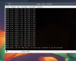
To check stability in an overclocked state, we used the Prime95 v.25.11 utility:

As practice shows, memory modules from different manufacturers, even with identical specifications, behave very differently when overclocked. Some react very sensitively to an increase in supply voltage, others do not, others allow you to greatly increase the frequency by just “loosening” the timings one step, and so on... Therefore, all the OCZ Blade rivals chosen for today’s comparison match it both in terms of operating speed and and by total volume. We meet:
1) Elixir M2Y2G64TU8HD5B-BD:

The cheapest kit of all participants, it is not even equipped with radiators. You can get acquainted with it in more detail from the article "".
2) GOODRAM PRO GP1066D264L5/4GDC:

Until now, this set has been the leader in terms of the totality of its overclocking characteristics. was also recently published on our portal.
Below are their main characteristics.
|
Model |
OCZ Blade Series OCZ2D1066LV4GK |
Elixir M2Y2G64TU8HD5B-BD |
GOODRAM PRO GP1066D264L5/4GDC |
|
Manufacturer |
OCZ Technology |
Nanya Technology |
Wilk Elektronik S.A. |
|
Set 2x2 GB |
2 sticks of 2 GB each |
set 2x2 GB |
|
|
PC2-8500 (DDR2 1066) |
PC2-8500 (DDR2 1066) |
PC2-8500 (DDR2 1066) |
|
|
Supply voltage |
|||
|
ECC/Buffered* support |
|||
|
Peculiarities |
Collapsible aluminum radiator |
Aluminum radiator |
|
|
Average retail price |
$100-125 |
||